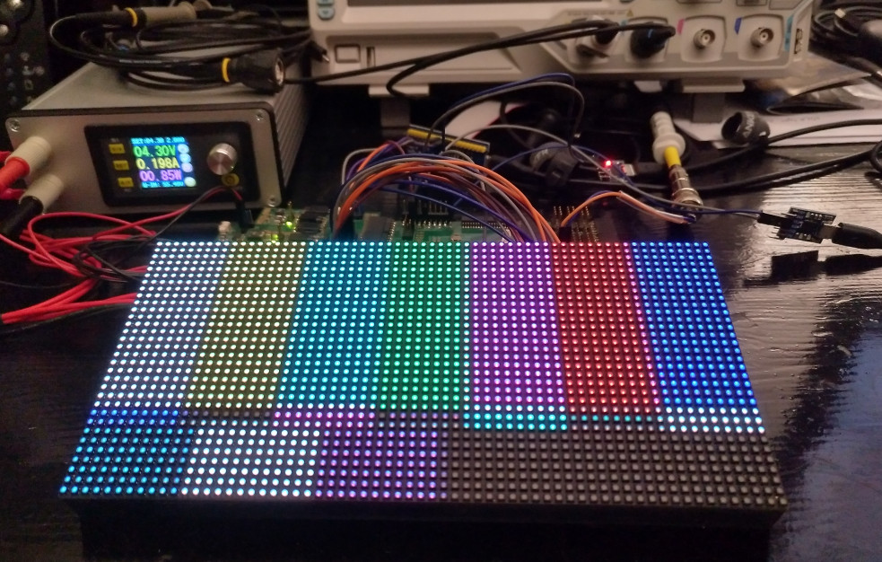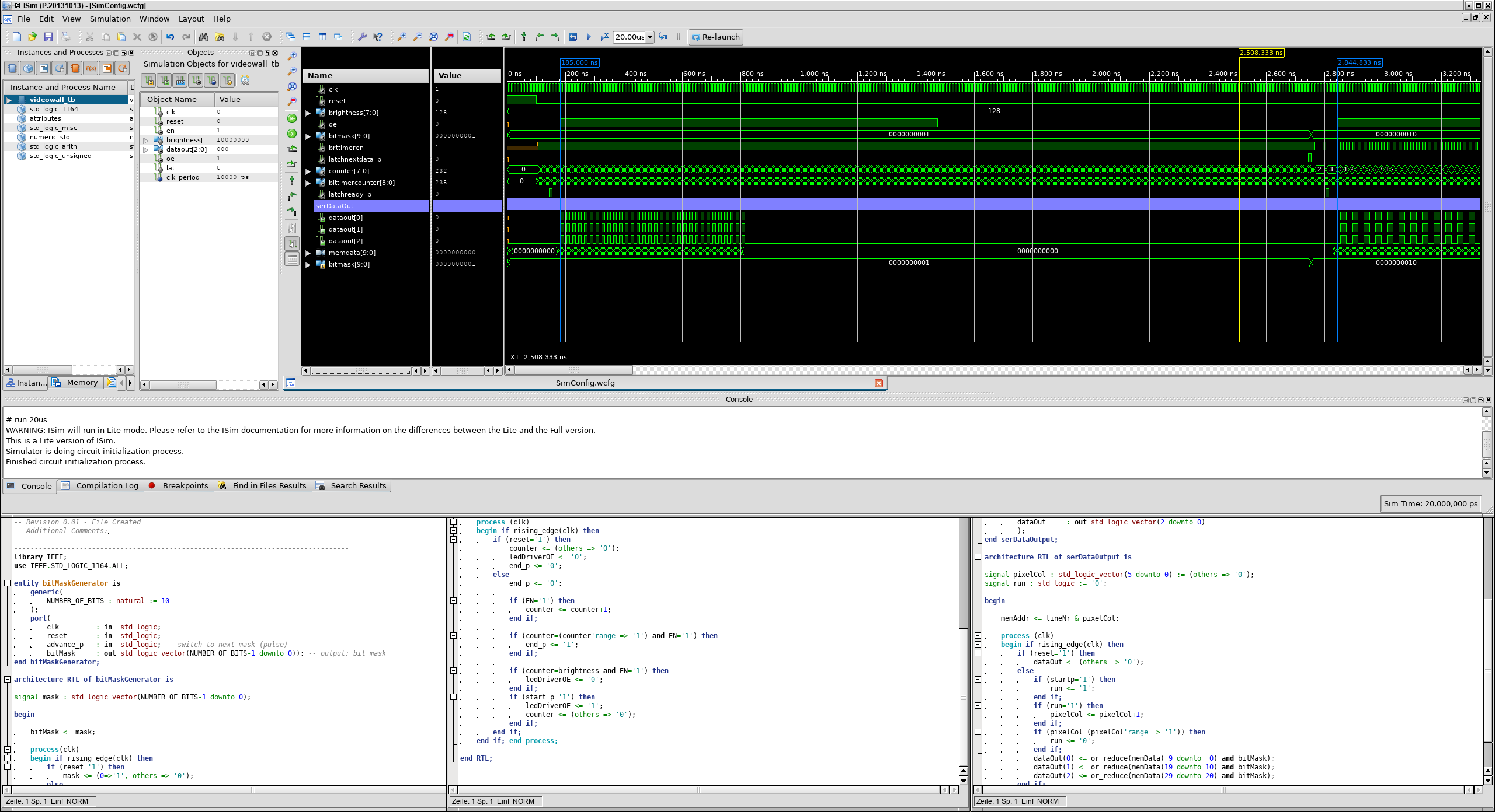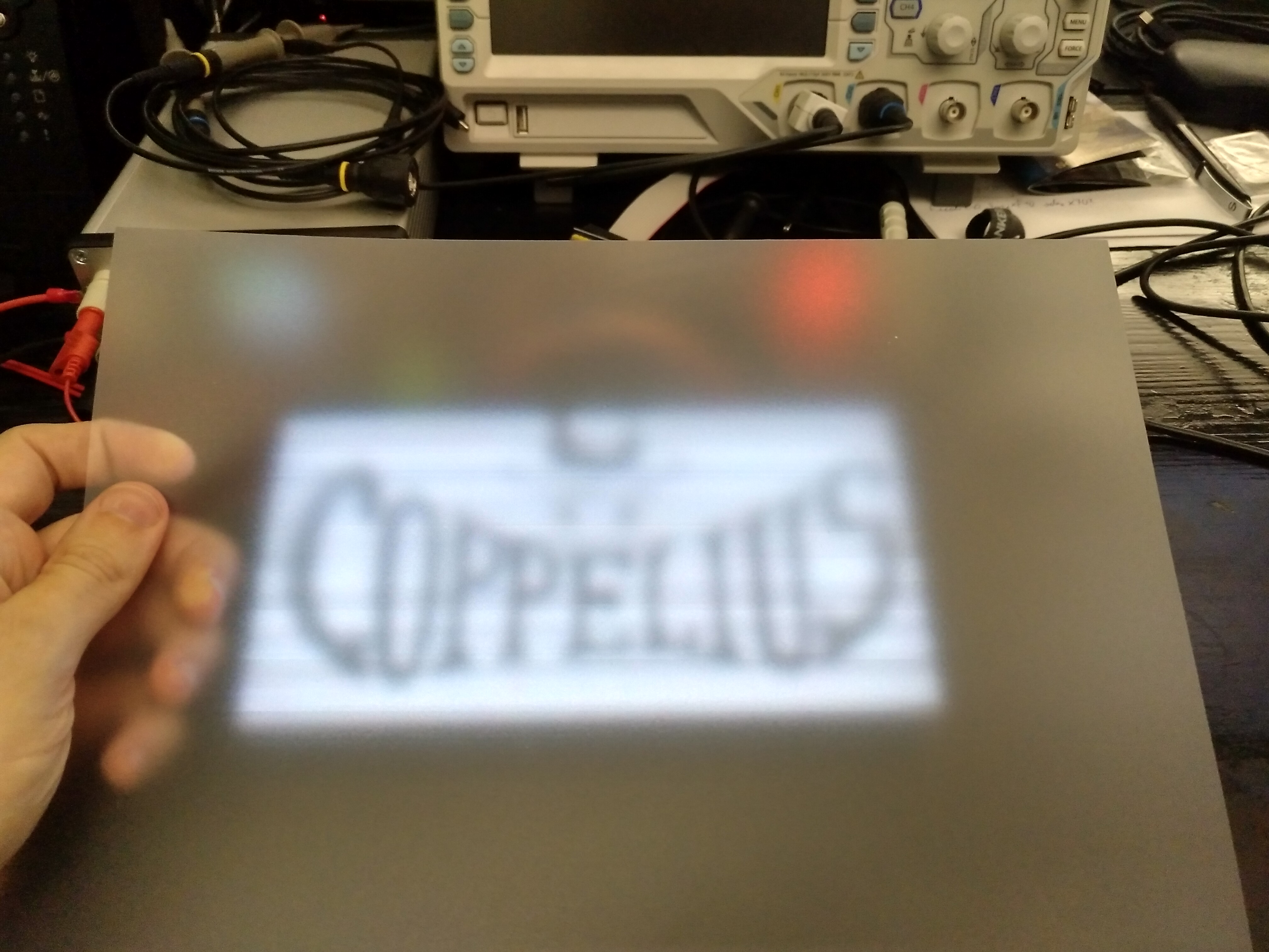
Just got all of my LED panel control scheme implemented and everything is working together nicely. Right now I am at 14+8 bit per subpixel (14 bit for each pixel and color + 8 bit for overall brightness). I am using line scrambling to increase the percieved steadyness of the image when the display is shaken (i.e. by walking).

Only 2% of the FPGA slices are used right now. The whole design runs at up to 375MHz, which is the maximum clock rate the global clock buffer of that FPGA offers. So my pipelining strategy works fine. The only limiting factor will be the amout of BRAM available, but I should be able to squeeze a dual buffer for the big display in with not too many tricks.
Next steps will be to decide on which panels to order and implementing an HDMI sink that then writes into the BRAM. Let’s see how difficult that is. The SERDES in my cheap FPGA can go up to 1GHz sampling rate, which limits me to 100MHz pixel clock. Should still be plenty, even if i have to simulate a 1280×1024 or bigger „monitor“. (Modern video sources don’t seem to handle screens with very low resultions all to well nowadays.)
